
Use of the Synopsys HAPS® FPGA-based prototyping environment
The Synopsys HAPS® System adds additional capabilities to the FPGA-based prototyping environments SoC Labs can use to support projects. The HAPS® system provides a greater amount of logic resources supporting development of larger SoC designs. It can be used to support multiple projects simultaneously. It is used by many semiconductor companies, including arm for their CPU verification. This collaboration project will use the HAPS® system in SoC Labs projects and share with the community experience in utilising such systems.
A Xilinx ZCU104 ZYNQ UltraSCALE gives a capable environment for developing the nanosoc reference design. As larger reference designs are developed they require larger FPGA-based prototyping environments to assist in their development. While a nanosoc based SoC design can be completed by a single person with a dedicated development environment, larger SoC designs require a team approach and a shared development environment. Team based development can use HAPS systems for a variety of roles in the SoC development cycle:
- verify the synthesizable RTL source code of larger SoC designs
- SoC Labs already uses a Continuous Integration and Deployment for verification approach where a virtualised environment builds the developing SoC design and regularly exercises it in a Design under Test environment. The HAPS system will improve this capability.
- support hardware/software co-design by supporting developers to write and test software on emulated SoC designs
Setting up the HAPS system
Synopsys provide a HAPS config tool to use with the HAPS system. This allows control of the system configuration, including power control of the HAPStrak expansion connectors, clock frequencies and enables, programming modes and reset control.
Programming the HAPS can be achieved in Xilinx Vivado, using the hardware server and the Xilinx virtual cable.
Debugging SoC's in HAPS
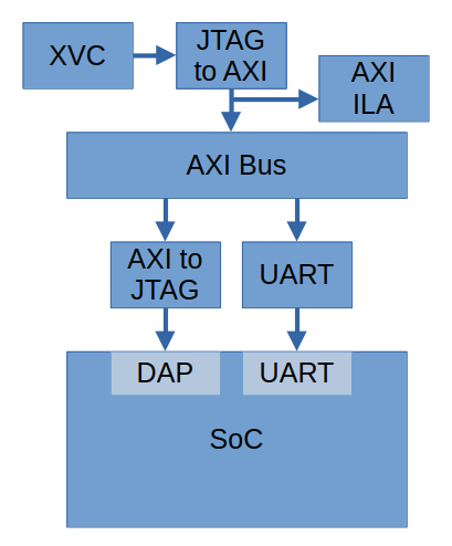
The Xilinx Virtual Cable (XVC) can be used for both hardware and software debugging of the SoC being emulated in the FPGA. The software debugging is achieved by using a JTAG to AXI bridge. This takes the JTAG from the XVC into a debug wrapper. Within the debug wrapper an AXI bus can be instantiated with various debug components. Below is diagram of a basic configuration with a JTAG component, which could be connected to the Debug Access Port (DAP) of the SoC and used for software debugging, alongside an AXI-UART component that can be used to read/write to the stdio of the SoC
The JTAG to AXI component can be controlled using TCL commands in the vivado hardware server. A simple example of this is shown below
reset_hw_axi [get_hw_axis hw_axi_1] # reset the axi component
set address 0xC0000000
set rt axi_bram_rt
set wt axi_bram_wt

# Setup read and write transactions
create_hw_axi_txn $rt [get_hw_axis hw_axi_1] -type read -address $address -len 4
create_hw_axi_txn $wt [get_hw_axis hw_axi_1] -type write -address $address -len 4 -data {44444444_33333333_22222222_11111111}

# Write data
run_hw_axi [get_hw_axi_txns $wt]

# Read data
run_hw_axi [get_hw_axi_txns $rt]
Using this approach, tests can be written in TCL to verify the system that is instantiated in the FPGA. The System ILA can monitor the AXI transactions, an additional ILA can monitor things like GPIO from the SoC.
Project Milestones
Do you want to view information on how to complete the work stage ""
or update the work stage for this project?
-
System Set Up
Target DateCompleted Date- Establish an initial knowledge base for the community on the HAPS system including set up requirements and other documentation
- Install the system as a network enabled service.
Result of WorkThe initial milestone to connect the HAPS as a network enabled service was completed by end of Sept 2024.
The task to establish an initial knowledge base for the community has not progressed due to other project pressures.
Our plan was to integrate the HAPS into the SoC Labs continuous integration / continuous deployment service. The next step was to deploy a SoC Labs reference design onto the platform. We achieved the later but outside of the CI/CD environment. This was to be the basis of the initial knowledge base for the community.
We will split these two tasks and close off this task.
-
Getting Started
Design FlowTarget DateThe guidance for the Getting Started milestone states it should help determine the best way to manage the project and to provides a simple way to manage the activities to be completed.
Project Management:
This project is not a System on Chip activity that follows the normal path of design flow steps. This project will selectively use some of the design flow steps and add some free form milestones as a way to guide the project to meet target dates to better drive the project to completion. As milestones are completed the date and details of the work need to be captured.
Design Method:
The project will use an agile method, with short development cycles, this will allow user needs to be established and then delivered. Agile usually defines a first iteration as a Minimal Viable Product.
Access to IP:
There are two aspects to this project:
- defining the IP needed from Synopsys for the HAPS operations
- defining an initial SoC design that will act as a reference model for deployment that can be used by the community as an example.
Synopsys IP:
SoC design IP:
Version Control:
Until a better alternative can be identified any materials developed by this project should be held in the SoC Labs git repository.
Project Structure:
This will need to be defined in more detail as we understand the use cases and information and other assets that need to be developed as part of the project.
The initial known outputs are:
- a knowledge base for the community on the HAPS system including set up requirements and other documentation
- a course on using HAPS as part of a real world System on Chip project.
Verification Methodology:
As outlined part of the project is to follow a typical SoC Labs reference design flow deployment using the HAPS to allow the three major uses of FPGA prototyping environments:
- verifying the synthesizable RTL source code
- integration into a Continuous Integration and Deployment service for team based projects
- support hardware/software co-design with test software on the prototype SoC design
-
Set Up Project in Version Control
Target DateSet Up a Project in the SoC Labs Version Control.
The project is using an agile method so the the project structure will evolve. An initial project structure should allow for the initial Minimal Viable Product deliverables:
a knowledge base for the community on the HAPS system including set up requirements and other documentation
a course on using HAPS as part of a real world System on Chip project.
Team

 Project Creator
 John Darlington
Community lead at University of Southampton
Submitted on
Comments
Hello
Hi, our university lab has both the HAPS environment and the Zynq 104 environment. Is there anything that can contribute to this project? What is the next milestone?
Hello and FPGA use in SoC Labs
Hi,
Thank you for your message and asking about the HAPS and other FPGA environments in use within SoC Labs. We use these environments in different ways for supporting the high level design prototype activities. One difference in our use is that we have worked to make the transition from FPGA to ASIC design as simple as possible. Usually people use the hard IP blocks in the PS side of the FPGA to do a lot of the functions in the SoC design and use the programmable logic (PL side) for just their specific project design. When people move to ASIC flow they need to replicate the hard IP blocks of the PS side. Our method is to use the soft IP from the Arm Academic Access early in the design and so use more of the PL and do not depend on the PS so much.
You can find some discussion of this in the nanoSoC reference design which we utilise the Zynq 104 board as a target for design activity. We also use the FPGA environments to establish Continuous Integration and Deployment for verification of our reference designs.
We will update the milestones here and look forward to collaborating with you.
Upcoming milestons
Hi, Thanks for getting in contact.
The development of the HAPS workflow has been on pause for a little while as we're getting ready for a tape out. However the plans we have in place are to first build an FPGA image using our nanosoc reference design as this has already been implemented on the zcu104 and other zynq platforms. The main goal for this effort is to work on the debug environment for a SoC
After that the plan is to use the system for the development of an A class SoC. First will be to implement the A53 subsystem that we have already developed and again ensure that we can successfully debug this in the HAPS.
Then we will use this to further develop the A53 subsystem into a full linux capable SoC; although this is likely to take some time.
If any of these are of interest to getting involved in, please let us know
Daniel
Add new comment
To post a comment on this article, please log in to your account. New users can create an account.