People


University of Southampton
|
Country
United Kingdom of Great Britain and Northern Ireland (the)
| |
| 34 | |
| 22 | |
| 7 | |
| Wed, 06/30/2021 - 14:50 | |
| AAA Member | |
Actions
Projects


The Synopsys HAPS® System adds additional capabilities to the FPGA-based prototyping environments SoC Labs can use to support projects. The HAPS® system provides a greater amount of logic resources supporting development of larger SoC designs. It can be used to support multiple projects simultaneously. It is used by many semiconductor companies, including arm for their CPU verification. This collaboration project will use the HAPS® system in SoC Labs projects and share with the community experience in utilising such systems.
 John Darlington


This collaboration project is aimed at providing specific tailored activities to the local geography in Canada by developing local actions that will help stimulate academics and their institutions and the broader semiconductor industry supporters to create new and exciting SoC design projects.
It may include holding specific local physical meetups where people can exchange design ideas.
It may include utilising locally provided routes to fabrication.
It may include sharing hard to locate test capability across academic institutions.
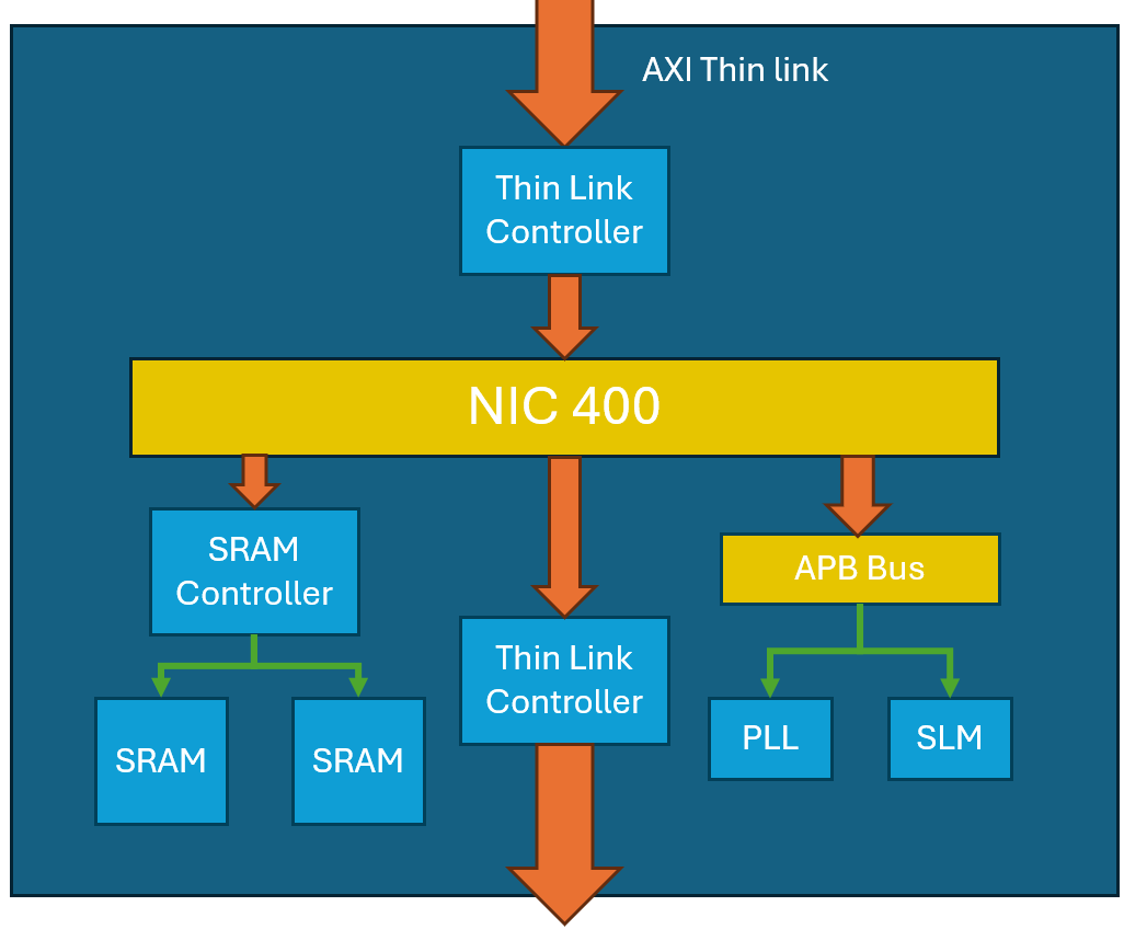

On-chip SRAM in ASICs can use a significant area, which equates to a significant cost. One solution is to make the memory off-chip. This project explores the use of Arm IP to create an SRAM chiplet design. The benefit is that standard memory chiplets can be fabricated at lower cost and used across multiple projects, miminising silicon area to the unique project needs.
 Daniel Newbrook
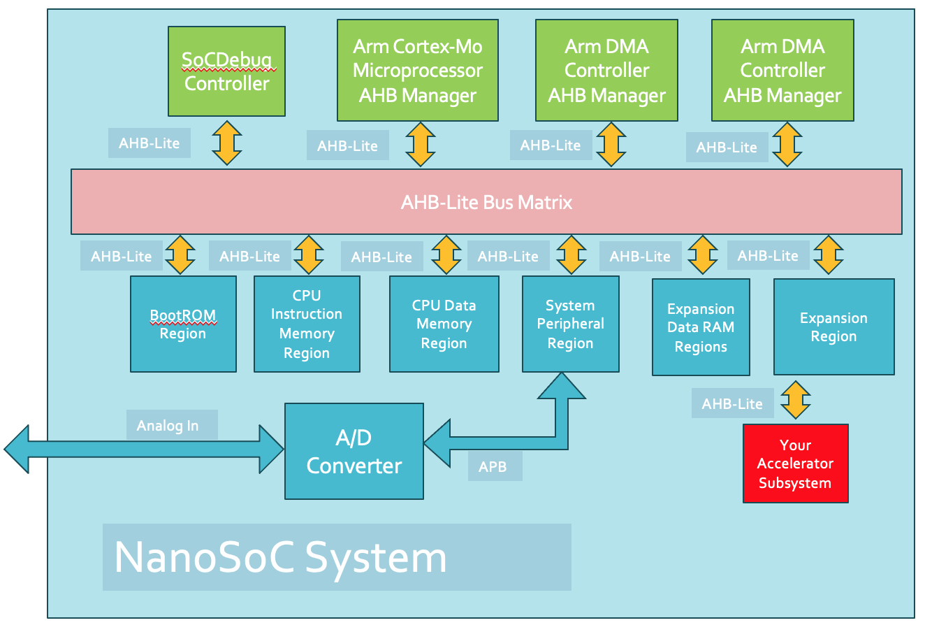
The aim of this project is to define a mixed signal subsystem for the nanosoc reference design.
The mixed signal subsystem should be able to sample analog signals at a regular sampling rate, and transmit a digital representation of this signal to the rest of the nanosoc system. In order to interface with real-world signals in a digital System on Chip ("SoC"), an analog to digital conversion ("ADC") is needed.